


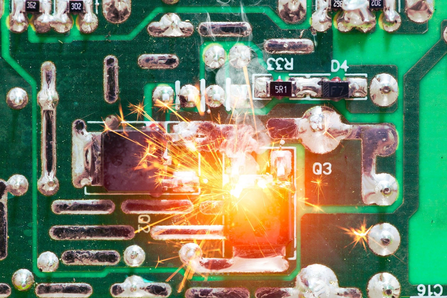

We encounter microelectronics in our daily life, waking up with the alarm on our smart phone, checking the news on a tablet, going to work with the car and working there on a laptop etc. All of these devices contain microelectronic components, making the devices “more intelligent” and their operation faster and more efficient. These microelectronic components produce heat under operation; this heat can hamper the performance and reduce the lifetime of the device. The award-winning work “A closer look at solder joints” - investigated the solder joints influence on the heat dissipation in microelectronic systems.
To minimize thermal problems, the evaluation of the thermal behavior and the heat dissipation optimization are crucial. The generated heat leads to a temperature gradient within the microelectronic component. Via heat conduction the generated heat is transported away from the interconnects through the printed circuit board.
The quality of the interconnects, like the amount of voids and the porosity in the solder joints, is essential for the quality of the heat dissipation and hence for the temperature of the microelectronic device. As the temperature of the component rises, the lifetime of the component shortens. At the Materials Center Leoben, the thermal design of the interconnects was evaluated and hence the systems can be optimized to avoid heat from harming the device and to improve the performance.
The miniaturization trend in the microelectronic industry lifts the thermal optimization onto a higher level. The reduction of package size and interconnection distance makes it more difficult to extract heat.
Hence, every part of a microelectronic system -ranging from the printed circuit board to the wafer level components - must be designed to optimize the heat dissipation. For this optimization, the knowledge of the devices’ thermophysical properties is essential.
Impact and effects
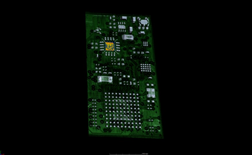
Nowadays, microelectronic components have dimensions in the nanometer to micrometer scale and consist of multiple thin-film layers. Conventional metrologies for bulk materials are usually unable to characterize their thermo-physical properties and to measure the heat flux across this length scales. Special metrologies, working in the time scales of nano-/picoseconds are required like the Time Domain Thermoreflectance (TDTR). This measurement technique is available at the Materials Center Leoben since 2018. The TDTR is a laser-based heating and sensing method to measure the thermophysical properties of thin films and their thermal interface resistance. It is based on the principle of thermoreflectance, allowing the detection of the thermal response of the heating event by monitoring the reflectance change. The understanding of the heat transport in the nanometer thin layers offers more insight in the generated heat and the temperature rise of the microelectronic system.
The goal of the Materials Center Leoben and its partners is to improve the thermal design of the microelectronic systems, to increase their lifetime and to make them more efficient.
Project coordination (Story)
Dr. Katrin Fladischer
Senior Scientist 3D Integration & Packaging
T +43 (0) 3842 45922– 533
Katrin.Fladischer(at)mcl.at
Project partner
Montanuniversität Leoben