


Advances in microelectronics
Technical devices are getting smaller while requirements in terms of reliability and function are increasing. This is presenting developers with more and more new challenges. Microelectronic devices have an impact on virtually all areas of life: they make everyday household tasks easier and enable communication and networking across the world, they control facilities and supply systems for power, oil, gas and water; support car, train and air travel and enable the most complex calculations.
A hidden interior
Microelectronic components always consist of a mix of different materials. And they are getting ever smaller in order to increase performance. One particular challenge for researchers is to characterise all the materials used in miniaturised microelectronic components.
In cooperation with its research partners, the MCL is thus developing efficient methods for measuring the structure and properties of materials in very small dimensions. The focus is on the structure, mechanical and electrical properties and residual stress. Geometric, mechanical and electrical properties of materials and specimens can be determined in the nanometre and micrometer range. The specimen thickness is often less than a tenth of the thickness of a human hair.
Limits of miniaturisation
The increasing miniaturisation is naturally raising new issues for developers. One example: many electronic components change when subjected to electric or thermal loads in service. In addition to changes in the material, cracks pose a particular problem because they form and grow when subjected to fluctuating temperatures. Mechanical failure caused by cracks is therefore a key cause of failure in technical devices. The MCL has comprehensive expertise to investigate the behaviour of cracks in inhomogeneous materials.
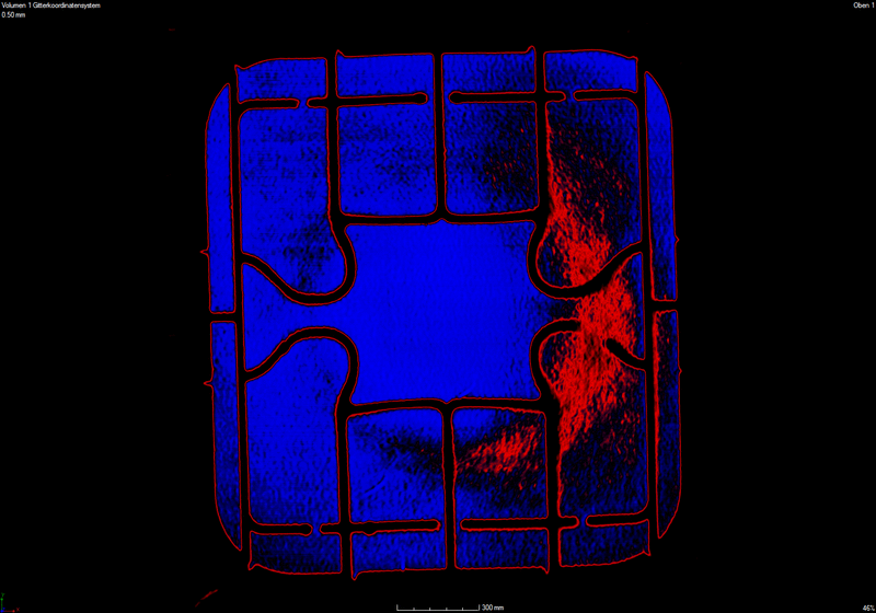
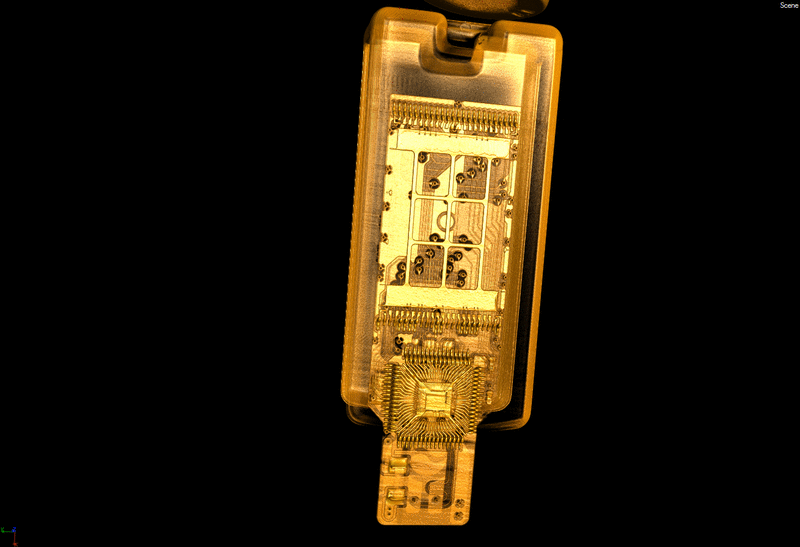
Three dimensional
Recently, the MCL invested in state-of-the-art equipment for the characterisation of the three-dimensional structure and damage behaviour of microelectronic components. One of these technical achievements is an acoustic microscope for analysing delamination in electronic components. The new CT scanner enables the analysis of three-dimensional structures with a resolution of up to 0.3 micrometres. The results achieved can be used to detect defects and develop three-dimensional models for finite element calculations.
Impact
The new infrastructure is being used for the development of new analysis methods. The first methods have already been successfully applied in R&D projects and are helping the MCL and its partners to gain a detailed understanding of damage processes in microelectronic components. The development of expertise in this area has already led to several EU projects.