


Through-Silicon Vias (TSVs) represent important parts for modern semiconductor technology. They are vertical tunnels (vias) that go through a silicon wafer. These vias help to make electronic devices smaller and more efficient by allowing three-dimensional integration. There are mainly two different types of TSVs - filled and unfilled. Each type serves a specific purpose in terms of conducting electricity and managing heat.
The choice of the TSV type depends on what the electronic device needs. Even though filled (closed) TSV designs have very low contact resistance, they suffer from a high degree of mechanical stress due to the mismatch of coefficient of thermal expansion between silicon and the filling material. Therefore, tungsten-lined unfilled (open) TSV replaces the closed TSV technology when thermal expansion is a concern.
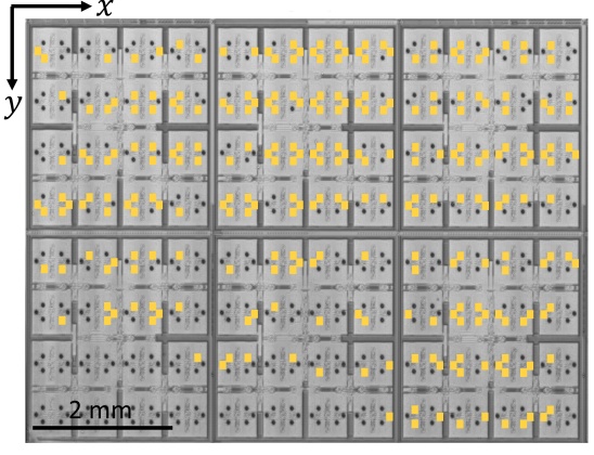
Each silicon wafer typically hosts around 100,000 of such open TSV structures. However, defects such as delamination, cracks or deposits can occur during the manufacture of these vias, which can significantly impair the performance of the component. This underscores the critical need for non-destructive, time-efficient, and cost-effective quality assurance and defect detection techniques close to the production line.
The Scanning Acoustic Microscope (SAM) is notable for its fast, cost-efficient, and non-destructive damage analysis of 3D interconnects. However, the achievable imaging resolution in SAM for failure analysis is related to the frequency of acoustic waves. There is a trade-off between resolution and penetration depth. Hence, a more innovative approach to detect deeper defects in TSVs with high resolution is essential.
With in the project REFORM, the researchers at MCL developed a SAM interferometry setup to detect defects inside the TSVs beyond its resolution limit by using special transducers and acoustic lenses.
The quality information about the TSVs is obtained in the form of interference SAM images. Additional scanning electron microscope (SEM) analysis helped to validate the acoustic interference image data.
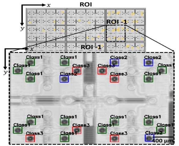
Furthermore, MCL developed an advanced deep learning model to automatically localize and classify defected TSVs. The developed deep learning method comprises a fully automated high-efficient End-to-End Convolutional Neural Network (E2E-CNN), utilizing two sequentially linked CNN architectures, suitable to classify and locate thousands of TSVs as well as provide statistical information (Fig.1).
Impact and effects
The unique workflow combining the utilization of interference-based experimental characterization and deep learning not only facilitates the efficient detection of defects inside the TSVs, but also gives the sufficient statistical information of defected TSV on the wafer-level. Furthermore, this specific analysis workflow developed at MCL is not only limited to SAM image data, but can also be applied to other classes of image data. This paves the way for an efficient fast inline feedback to the production.
Published in: P. Paulachan et al. An end-to-end convolutional neural network for automated failure localization and characterization of 3D interconnects. Sci Rep 13, 9376 (2023).
Project coordination (Story)
Roland Brunner
Gruppenleiter Material and damage analytics
Materials Center Leoben Forschung GmbH
Roseggerstrasse 12, 8700 Leoben
Roland.Brunner(at)mcl.at
IC-MPPE / COMET-Zentrum
Materials Center Leoben Forschung GmbH
Roseggerstrasse 12
8700 Leoben
T +43 (0) 3842 45922-0
mclburo(at)mcl.at
www.mcl.at
Project partners
• PVA TePla Analytical Systems GmbH, Germany
• ams-OSRAM AG, Austria
• Materials Center Leoben Forschung GmbH, Austria