Electron Microscopy Laboratory

The core competencies of the electron microscopy laboratory lie in the investigation of material and fracture surfaces by means of high resolution scanning electron microscopic methods. For target preparation and local 3D microstructure tomography a focussed ion beam system is available.

Our main focus is on:

  • SEM-characterisation of surfaces, fracture surfaces and metallographic sections
  • Local cross-section-preparation by means of SEM-FIB and analysis in high resolution SEM
  • Material investigations including 3D microstructure tomography by means of SEM-FIB technique
  • Target preparation of TEM thin films and atom probe specimens for subsequent high resolution analyses
  • Deformationless cross-section and plane preparation by means of ion slicer
  • Material characterisation with reference to damage


The range of services of the scanning electron microsopy laboratory extends from quick standard analyses to sophisticated high resolution examinations using the latest analysis technologies available in the field of cross-beam scanning electron microscopy.

Our Range of Services

  • Material characterisation by means of scanning electron microscopy (SEM) (e.g. microstructure assessment, phase composition)
  • 3D characterisation of component and fracture surfaces incl. determination of local chemical composition and damage
  • 3D microstructure tomography based on grain orientation or chemical composition
  • Target preparation of atom probe specimens from arbitrary areas of samples (bulk materials and thin films) for subsequent analysis in cooperation with our research partners
  • Target preparation of thin films for transmission electron microscopy (TEM)
  • Production of micro specimens for mechanical in-situ tests with different geometries (e.g. cuboid, cylinder or micro tensile and bending specimens) for subsequent testing in cooperation with our research partners
  • Introduction of small crack-like defects (in the sub-µm to µm range) for investigation of the behaviour of short cracks


Our Equipment

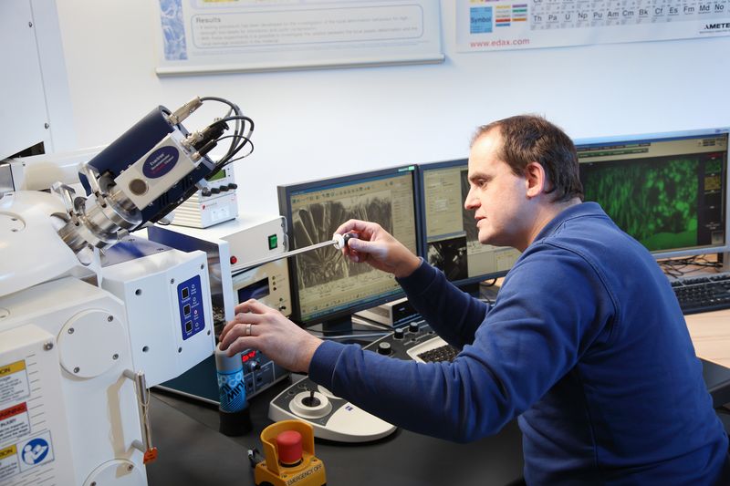
Cross-beam scanning electron microscope with focussed ion beam (FIB) from Zeiss (AURIGA®-CrossBeam® Workstation):

  • High resolution field emission scanning electron microscope with various detectors (secondary electron, backscattering electron, STEM, secondary ion, in-lens and EBSD detector)
  • Focussed ion beam (Cobra-Orsay-Physics)
  • Gas injection system for different substances (for deposition of graphite or platinum, for etching by means of iodine and water vapour) and charge compensation for analysis of non-conducting specimens
  • Energy dispersive X-ray analysis system (EDX)

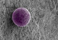
Scanning electron microscope with large specimen chamber from Zeiss (EVO MA 25®):

  • Scanning electron microscope with LaB6 cathode and low pressure mode (also suitable for analysis of non-conducting and contaminated (e.g. oil contaminated) specimens
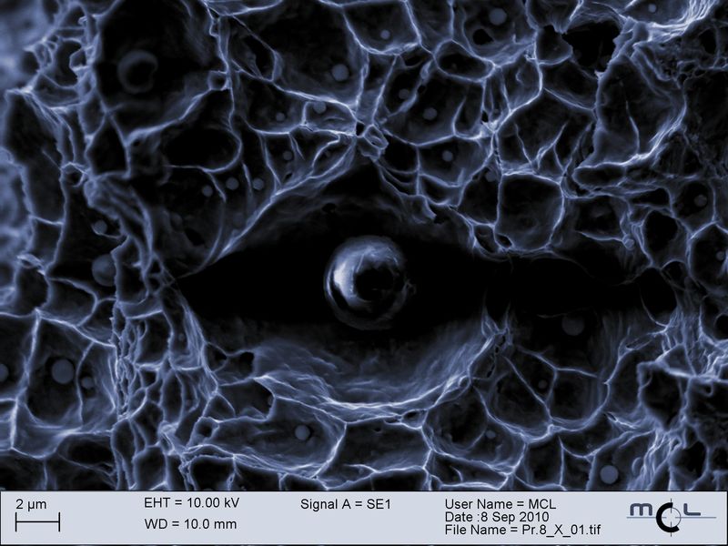
  • Large sample chamber for the analysis of components and large specimens: specimen weight with full tilting capability up to 2.5 kg, specimen height up to ~ 100 mm; specimen weight without tilting > 5 up to ~ 10 kg (max. height up to ~ 210 mm)
  • Secondary and 5 quadrant backscatter electron detector
  • Energy dispersive X-ray analysis system (EDX)
  • 3D surface topography software from Alicona (MeX)