Simulation and modeling of materials for microelectronics
Our research activities comprise the modeling of microelectronics components, with a strong focus on multi-scale and multi-physical material behavior. One of the main topics is transient-thermal transport, taking into account complex damage formation under thermo-mechanical load. For this task advanced damage and fracture mechanical concepts are used.
Both, the detection of damage (key word: “Non Destructive Testing”) and also the modeling of the material behavior requires increasingly complex mathematical solution methods and direct as well as inverse numerical modelling techniques.
Damage in multi-material composites
One of our major interdisciplinary research activities is the modelling of damage in multi-material composites in microelectronics. First our approach starts from the fundamental question: “What is damage?” ending in the extremely application oriented question: “How can one avoid it?”. Here we follow a material oriented approach, requiring advanced experimental as well as modeling techniques.
Standard fracture mechanical methods are limited in applicability if the crack approaches surfaces and interfaces. Recognizing this fact, Simha at al. and Kolednik et al. in cooperation with the MCL have developed, and constantly evolved, the “Configurational Force” concept. With that method the crack driving force can be computed correctly even if the plastic zone extents to the surface or across interfaces [2,3]. Engineering of new fracture tough components and sophisticated fracture experiments are supported in a founded theoretical manner by this approach.
This allows e.g. the design of thin layered systems with significantly enhanced fracture toughness compared to homogeneous bulk material [4,5]. This is inspired by nature. E.g. nacre has a natural microstructural design, giving it a fracture toughness many orders of magnitude higher than its very brittle constituent material calcium carbonate [6].
Thermal Management
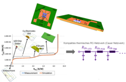
Thermal transient simulation, in combination with experimental thermal impedance analysis, and the use of the so-called structure function enables deeper understanding of the thermal behavior of microelectronics components. The structure function is a mapping of the heat path from heat source to heat sink in the form of thermal resistances and capacities. Comparison of simulated and measured structure function constitutes an advanced tool for validation of the simulation and the interpretation of the experiment. By this means improvement of the thermal management of microelectronics by “Virtual Prototyping” is enabled [1].
In this way we e.g. develop special PCB concepts including high thermal conductive but electrical insulating ceramic coatings at critical points within the system. Analyzed compact thermal models in addition can improve the “Condition Monitoring” and “Structural Health Monitoring” of components. This is considered as an innovative and cost effective method for “Predictive Maintenance” e.g. in lighting industry.
Simulation enabled materials characterization
The material characterization accompanied by simulation is used in “Non Destructive Testing” using ultrasound and also for material-parameter determination like: eigenstress, elastic constants, flow curves, fracture- and interface properties, thermal conductivity and capacities. In particular numerical modeling is used to go beyond analytical evaluation methods for micro pillar, Raman, XRD, nanoindentation etc. experiments.
Ultrasound simulation
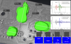
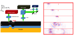
Ultrasound simulation is used to support our experimental methods: the “Scanning Acoustic Microscope (SAM)” at MCL and the “Laser Ultrasound Method” in cooperation with the Karl-Franzens-University Graz. The combination of simulation and experiments gives an advantage especially for the interpretation of complex sound wave behavior like propagation and conversion of bulk and surface waves. This enables an advanced interpretation an detection of defects in complex microelectronics components [1,2] and the characterization of elastic parameters e.g. of thin films [3,4].
One methodological focus lies in the use and development of the “Elastic Finite Integration Technique (EFIT)” capturing the behavior under strong damping, dispersion and transmission in complex microelectronics components.
Eigenstress
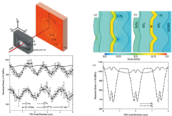
Eigenstresses in thin layers take on very high values (in the order of GPa). The stored elastic energy can constitute a major crack driving force. In Leoben the “Ion Layer Removal (ILR)” method was developed, which enables the determination of local and depth resolved eigenstress measurements [5]. By supportive finite element modeling (FEM), stress reconstruction is also possible in the presence of anisotropy and plasticity.
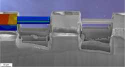
FEM is also used in combination with Raman measurements to reconstruct the complex stress-tensor field within microelectronics components, e.g. for 3D integration [6]. The simulation of layer per layer deposition, including intrinsic and thermal stress, was used to understand the stress concentrations at the scalloped wall of a tungsten Trough Silicon Via (TSV) (because of the Bosch process), which was measured by X-ray nanodiffraction [7].
Fracture- and interface-strength of thin films
Fracture and Interface toughness is strongly dependent on the microstructural design. To investigate this topic further, simulations and micro-cantilever fracture experiments are done. For this task the “Configurational Force” concept is used (see also “Damage in multi-material composits”) [8].
Publications
Damage in Multi-Material Composites
- J. Magnien, J. Rosc, M. Pfeiler-Deutschmann, R. Hammer, L. Mitterhuber, S. Defregger, F. Schrank, E Kraker, Accelerated thermo-mechanical test method for LED modules, Mechanical and Multi-Physics Simulation and Experiments in Microelectronics and Microsystems (EuroSimE). IEEE (2016)
- N.K. Simha, F.D. Fische, G.X. Shan, C.R. Chen, O. Kolednik, J-integral and crack driving force in elastic–plastic materials, Journal of the Mechanics and Physics of Solids 56 (2008) 2876–2895
- W. Ochensberger, O. Kolednik, Physically appropriate characterization of fatigue crack propagation rate in elastic–plastic materials using the J-integral concept, International Journal of Fracture 192 (2015), 25-45
- O. Kolednik, J. Predan, R.D. Fischer, P. Fratzl, Bioinspired Design Criteria for Damage-Resistant Materials with Periodically Varying Microstructure, Advanced Functional Materials (2011), 3634-3641
- M. Sistaninia, O. Kolednik, Effect of a single soft interlayer on the crack driving force. Engineering Fracture Mechanics 130 (2014) 21-41
- L. B. Freund and S. Suresh, Thin film materials: stress, defect formation and surface evolution, Cambridge University Press (2004)
Thermal Management
- L. Mitterhuber, S. Defregger, R. Hammer, J. Magnien, F. Schrank, S. Hörth, M. Hutter, E. Kraker, Investigation of the Temperature-Dependent Heat Path of an LED Module by Thermal Simulation and Design of Experiments, Therminic 2016, 22nd International Workshop Thermal Investigations of ICs and Systems.
Simulation Enabled Materials Characterization
- E. Grünwald, J. Rosc, R. Hammer, P. Czurratis, M. Koch, J. Kraft, F Schrank, R. Brunner, Automatized failure analysis of tungsten coated TSVs via scanning acoustic microscopy, Microelectronics Reliability (2016)
- E. Grünwald, R. Hammer, J. Rosc, G. A. Maier, M. Bärnthaler, M. J. Cordill, S. Brand, R. Nuster, T. Krivec, R Brunner, Advanced 3D Failure Characterization in Multi-Layered PCBs, NDT&E International 84 (2016) 99-107
- E. Grünwald, R. Nuster, R. Hammer, H. Aymann, G. Paltauf, R. Brunner, Characterization of polyimid-multi-layer thin films combining laser ultrasonic measurements and numerical evaluations, 17th International Conference on Thermal, Mechanical and Multi-Physics Simulation and Experiments in Microelectronics and Microsystems (EuroSimE). IEEE (2016)
- E. Grünwald, R. Nuster, R. Treml, D. Kiener, G. Paltauf and R. Brunner, "Young’s Modulus and Poisson’s Ratio Characterization of Tungsten Thin Films via Laser Ultrasound," Materials Today: Proceedings 2, p. 4289 – 4294, 2015
- R. Schöngrundner, R. Treml, T. Antretter, D. Kozic, W. Ecker, D. Kiener and R. Brunner, "Critical assessment of the determination of residual stress profiles in thin films by means of the ion beam layer removal method," Thin Solid Films 564, pp. 321-330, 2014
- M. Deluca, R. Hammer, J. Keckes, J. Kraft, F. Schrank, J.Todt , O. Robach , J-S. Micha, S. Defregger, Integrated experimental and computational approach for residual stress investigation near through-silicon vias, submitted to Journal of Applied Physics (2016)
- J. Todt. H. Hammer, B. Sartory, M. Burghammer, J. Kraft, R. Daniel, S. Defregger, X-ray nanodiffraction analysis of stress oscillations in a W thin film on through-silicon via, Journal of applied crystallography 49 (2016)
- R. Treml, D. Kozic, R. Schöngrundner, O. Kolednik, H.-P. Gänser, R. Brunner, D. Kiener, Miniaturized fracture experiments to determine the toughness of individual films in a multilayer system, Extreme Mechanics Letters (2016)


![Simulation for the development of accelerated life tests and substitution by mechanical tests. Led module with wire-bonds (upper picture). FEM simulation of temperature cycle tests (lower left) and FEM do develop substituting, alternative tests [1].](/fileadmin/_processed_/5/7/csm_Simul_FE_Zuverlaessigkeit1_6d4e928395.png)
![FEM simulation of plastic zone at a crack approaching the surface of a material [2].](/fileadmin/_processed_/6/d/csm_Simul_FE_Zuverlaessigkeit2_b75f288f36.png)
![Fracture experiments and simulations (using the “Configurational Force” concept) for micro-cantilevers [8].](/fileadmin/_processed_/3/e/csm_Simul_FE_Zuverlaessigkeit8_fee78781da.png)