


Microelectronics Rethought at the MCL
"Our knowledge comprises everything from the structure and properties in a nano scale to the performance of electronic devices."
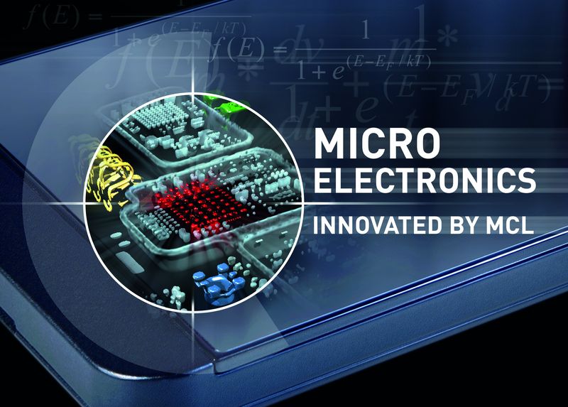
More and more functions and a higher performance packed into smaller devices: that’s where microelectronics is heading. This involves hugely varied classes of materials combined in small spaces and ultra-thin layers and under increasing extreme conditions. Mechanical, electrical, and thermal stresses on material composites have an increasing impact on the durability and security of microelectronic devices whose range of functions is also expanding through the integration of modern sensors. The MCL combines materials knowledge, process technology, analysis, and simulations to contribute to ongoing innovation.
Highest Perfection on Smallest Space.
")
Materials research at the nano and micrometer scale is becoming more and more important. It helps guarantee the performance and reliability of microelectronic components in order to manufacture new functional sensor systems. By miniaturising electronic components whilst simultaneously increasing their functional range the mechanical, thermal, and electrical stresses on the materials involved continue to grow, and may eventually lead to the failure of the component. At the same time, nano materials are opening up new applications. Th research at the MCL ensures that innovative and highly reliable components can be implemented quickly, thus reducing the associated development costs.
Processes
"Step by step to perfection."
The MCL has an extensive range of methods and wide-reaching knowledge of process technology in the manufacture of electronic components. We offer two different approaches to provide our partners and clients with the best possible assistance:


First, we support industrial processes by determining the stresses to which materials and components are exposed during manufacturing. This includes, for example, examining the development of internal stresses and how they are related to the design of the component using complex process simulations.
Second, for joint process and material developments, the MCL has access to a process chain for developing gas sensors on Si-chips at its site in Leoben and at a cooperative site in Vienna. Here the focus is on innovative materials for sensor technology and sensor manufacturing using CMOS-compatible technologies.
Supporting technologies:
Packaging and embedding | Bonding | Through-silicon vias | Process modeling of mechanical and thermal loads for design optimisation
Technologies on site:
Spray pyrolysis | Process chain for thin-film and nanowire gas sensors on 8 inch wafers | Structuring
Reliability and System Performance
"Preconditions for reliability."
The MCL offers a variety of testing methods to determine the durability of electronic components. The focus lies on identifying the thermal, electrical and mechanical properties of components and their constituent materials. With the aid of advanced numerical analysis, we close the circle between function assessment, reliability assessment, and predictive reliability analysis. These findings form the basis for designing new and reliable products.


Key Topics
3D-integrated components and systems | Thermal assessment of packages | Nanosensor development
Test Methods
Thermomechanical tests | Electronic tests | Combined mechanical, thermal and electrical test methods | Determination of residual stress within the package using XRD
Analytical Methods
Non-destructive characterisation using computed tomography and acoustic microscopy | Destructive characterisation using target preparation, optical microscopy, scanning electron microscopy with focused ion beam-technology, electron backscatter diffraction | Material characterisation using indentation methods and scanning force microscopy | Material characterisation using microdynamicmechanical analysis | Sensor test bed
Simulation Services
Material modelling – development of material models | Modelling of mechanical and thermomechanical loading | Interfaces | Modelling of crack formation and growth | Design optimisation in terms of thermal management and stress
Examples
"We are designing nanosensors for microelectronic components."
The MCL is coordinating an EU project with 17 partners aimed at integrating nanosensors into microelectronic components. The primary objective is to develop extremely small sensors for integration into computer chips. Innovations such as these could be used in smartphones, for example, to warn participants in outdoor sports of dangerously high ozone levels, city dwellers of high levels of particulate matter, farmers of gases in silos, or sunbathers on the beach of dangerous exposure to UV radiation. Nanosensors also open up new possibilities in building technology: networks of infrared sensors can locate the source of a fire and indicate the exact location of potential victims. Additionally, nanosensors enable the control of air conditioning systems based not only on room temperature but also on the CO2 concentration, helping to make them more energy-efficient.