


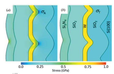
Thermal and residual stresses on semiconductors have a major influence on the yield during processing and the reliability during application. This is especially valid for modern 3D integrated devices where through silicon vias (TSV) are used to connect the front side with the backside. Such structures have a layer wise build up with thin coating made from different material classes. When, for example, a stack of SiOx, Ti, TiN and W is produced, residual stresses develop in all layers.
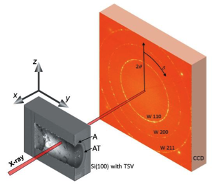
Spatial resolved characterization of residual stresses structure components can be analysed using nano-beam X-Ray diffraction. With this method MCL together with researchers from university of Leoben and Erich Schmid institute were able to characterize the stress profile in a TSV. Together with the so called Ion Layer Removal method the stress state in plane and out of plane could be determined.
Finite element simulations were not only used to determine effects of sample preparation and recalculate the experiments but also to build up a design tool for construction of stress reduced stacks.
Contact: Elke Kraker