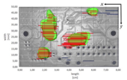
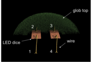
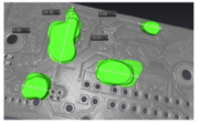
The characterization of elastic material's properties in thin film systems or the non-destructive identification of failure modes in highly complicated 3D integrated structures or modern print circuit boards (PCBs) with respect to “rapid learning” represents a demanding challenge in microelectronics. Ultrasound waves are a highly efficient possibility for the non-destructive characterization of material properties and failures in microelectronics. Here, image as well as non-image based methods can be used.
Examples are scanning acoustic microscopy (SAM) or laser induced ultrasound (LUS), respectively. The MCL develops in collaboration with partners e.g. PVATepla, Fraunhofer IMWS, and the Imec novel measurement and analysis approaches which are based on the SAM method. In addition, novel concepts for non-contact characterization of material parameters using laser induced ultrasound are developed in collaboration with the University of Graz. The goal is to provide accurate process attendant failure and material characterization.
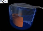
The analysis of complex and small geometries used in e.g. microelectronics or modern energy storage systems is highly demanding. Here, tomography based methods like X-Ray computed tomography (XCT), FIB-tomography etc. represent highly useful tools. However, the analysis of the obtained 3D data to gain accurate information is an obstacle due to reconstruction problems, measurement artefacts, limited resolution, and contrast. In order to meet these challenges the MCL develops algorithms for demanding segmentation problems, applies commercial available state of the art software packages and uses tomography based methods to produce reliable data. In addition, the MCL uses data meshing approaches where 3D & 2D image data is linked to numerical simulations like CFD and FEM to provide simulations on realistic samples. The overall goal is to provide a comprehensive, extensive, fast, and reliable information regarding structural properties for material engineering.
Contact: Roland Brunner


