


Product Development in Microelectronics
The MCL research in microelectronic product development is directed towards
- miniaturised sensor systems
- new product designs to enhance the reliability of microelectronic compunds
Sensors for the Consumer Market

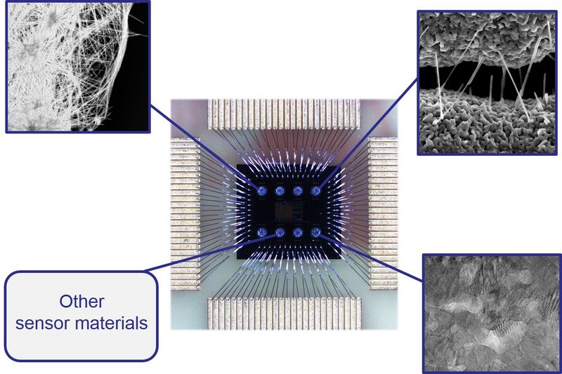
Nano technology based sensors that are integrated on CMOS based electronics devices to offer new possibilities in gas sensing for consumer applications. To achieve this goal metal oxide nano wires are functionalised in order to become more sensitive to various gases.
Together with company partners such as ams AG and EVGroup an innovative process chain is developed to apply nano wires and nanoparticles on CMOS-wafers to transpose the distinguished properties of nano-components in gas-sensor-technology, concerning both technical and economic aspects.
High-sensitive sensors by use of nanowires and nanomaterials
Within the scope of international projects like MSP the MCL is working with its partners to develop new sensor systems and production technologies, which should enable a flexible "Plug-and-play" 3D-integration of nano sensors and nanotechnological components on CMOS-chips to produce high-sensitive sensors which are equally capable for bulk production.
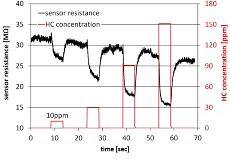
Embedded pattern recognition for MOx gas sensors
Most gas sensors are not only sensitive to a specific gas, but also to other gases, temperature and humidity. This gives a most complex calibration function requiring efficient implementation. Furthermore, sensor response to temperature transients has been found to be information-rich, significantly increasing typical sampling frequencies. Interpretation requires pattern recognition and efficient implementation thereof. In the FP7 project Multi-Sensor Platform (MSP), respective sensing units have been built and explored. In this sub-project, interpretation of recorded data is investigated and the potential for real-time implementation is explored.
Environmental monitoring
Sensors for environmental monitoringwill be widely used in future - in order to alert people from the existence of hazardous gases such as ozone, carbon monoxide or from high fine dust contents in the air.
Contact: Anton Köck
Reliability and Design of Packages
In-situ-characterisation of white-light LED modules by computed tomography during thermal cycling
The application of light-emitting diodes (LED’s) is growing fast mainly because of their high efficiency compared to classical filament lamps. Nevertheless, there are still some challenges to overcome. In particular, the LED modules wirings are areas of high thermo-mechanical stress.
To design the connection wires accordingly, the exact load of material-composite needs to investigated. Development goals are to further increase the illumination density, and the efficiency while ensuring a high colour quality and life time of LED modules. Thermal- and thermo-mechanical management of LED modules is one of the solution paths to meet these goals.
Simulation of thermo-mechanical loads of LED-modules
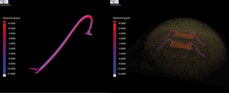
Together with Tridonic Jennersdorf GmbH the Materials Center Leoben investigates thermo-mechanical problems in white-light LED modules applying experimental methods as well as numerical simulations. The goal is to increase the lifetime of LED modules. A new method was developed, which allows recording and analysis of images made with computed tomography (CT-images) as a function of temperature. The combination of both CT-analysis and thermo-mechanical simulation enables a detection of stress localisations in the module which provides a valuable basis for module optimization.
Thermal Management in high power LEDs
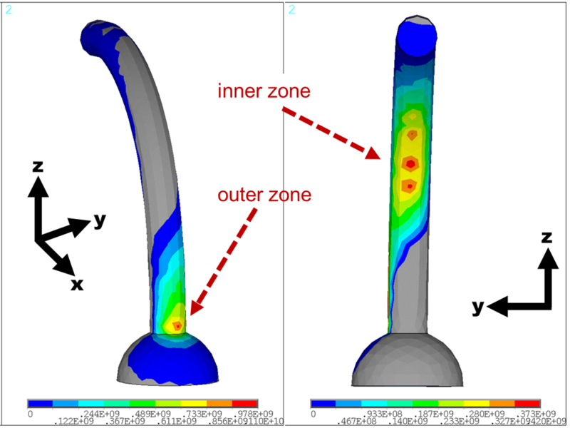
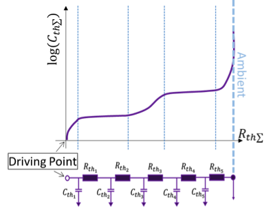
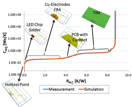
One key aspect in light emitting diode (LED) systems engineering is about understanding and management of the heat transfer during device operation. A deeper idea of the thermal behavior of an LED module can be gained by an in-depth thermal path analysis. The three-dimensional heat path of the LED is influenced by its operating conditions (e.g. heat sink temperature, driving current, the properties of the thermal interface materials of the device attachment to the heatsink). Analysis of heat transport in LED modules as well as in other electronic packages can be performed using the so called thermal impedance analysis combined with heat transport simulations.
With this Method, various loadings from application can simulated and the influence on the heath path and the temperature dependencies of the used materials can be determined. For the analysis, the measured signal is transferred in a network of thermal resistances and thermal capacitances and the same network is used for simulation the properties. By comparing experimental and calculated structure function the simulation model can be validated in a reverse engineering approach. The LED devices simulation model is generated according to its geometric buildup and a simulated structure function is derived therefrom. These validated models can now not only be used for Design of Reliable components and material optimization but also for condition monitoring of LED Systems.
Online Power LED Lifetime Monitoring (OPAL)
Thermal transients as observable when switching LEDs on or off allow - under certain constraints - for a detailed in-situ characterisation of thermal interfaces. In the present internal project, integration of both measurement electronics and signal processing in a portable device was investigated. LEDs were monitored in operation and transients were extracted. The developed platform allows for enhancing lab-based quality control procedures as well as field measurement campaigns. Wireless communication enables fully autonomous units.
Contact: Elke Kraker