


Process Development for Microelectronic Devices

In our division process engineering we deal with packaging of electronic compounds and with new and innovative methods and processes for the production of nano-electronic systems.
Packaging of Electronic Components
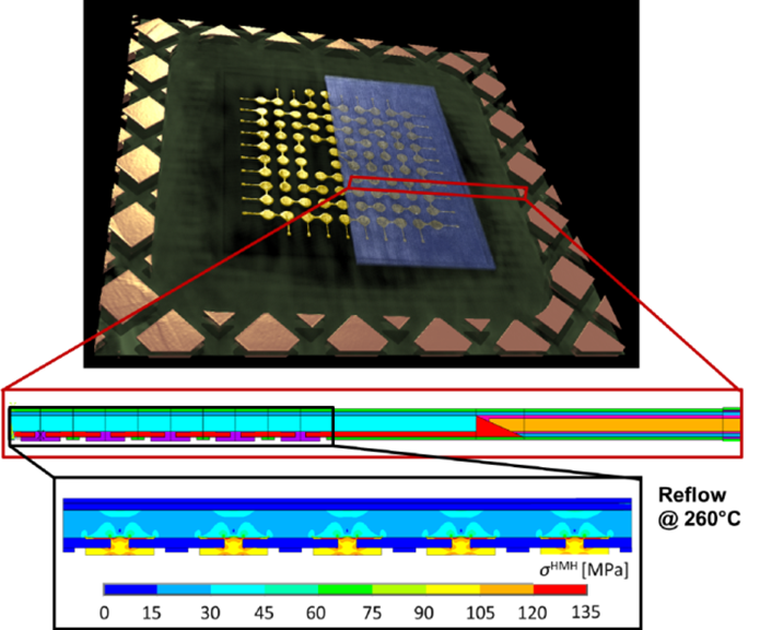
The final step in the production of electronic parts is the packaging and wiring of components. During these processes, the finished and tested components are soldered, glued, connected, and encapsulated very often in polymer based materials. All of these steps bring additional loading to the component due temperature treatments and different coefficients of thermal expansion. These loads can either directly lead to the component failure or to permanent deformations and stresses that affect the long-term behaviour of microelectronics components.
An example of a manufacturing process is the embedding of micro-electronic components in printed circuit boards. The image shows a Si-Chip, which has been integrated into a circuit board by means of a multi-stage embedding process. Each of these steps causes thermo-mechanical stresses. The aim of this study is to predict the stress on the component in order to minimize it by optimizing the production process and the component geometry.
Contact: Elke Kraker
Development of New Industrial Processes for Nano-Electronics
The fabrication of functional coatings and nanowires for gas sensing on CMOS chips requires special reliable processes that enable fabrication below 400°C. At the MCL spray pyrolysis is used to develop and fabricate special thin film metal oxides (MOx) and transfer processes for nanowires and nanoparticles are brought together with partners to a serial production status. Spray pyrolysis is method to produce very thin films metal oxide (30-100 nm). For that, a precursor solution is sprayed on a up to 400°C hot surface.
In the framework of national and international projects the technology for production of Tin-, Copper- and Zincoxides is engineered and optimized. Together with partners a process tool is developed to enable future application on 200 mm Wafers.
Contact: Anton Köck