


The core competence of the laboratory for microelectronics is the characterisation of microelectronic components and materials for these components.
The staff members of the laboratory for microelectronics are your qualified partners concerning materials in electronic components and systems, non-destructive testing and miniaturised systems.
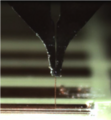
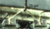
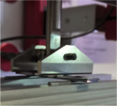
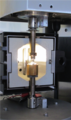
Mechanical Testing / Bond Tester
We characterise the mechanical properties of different materials used for the manufacturing of microelectronic components as well as simple and complex components.
Our main focus/competences
-
Determination of interfacial resistances on different materials via shear tests, peel tests, double-cantilever beam tests
-
Reliability tests (creep tests, cyclic loading)
-
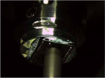
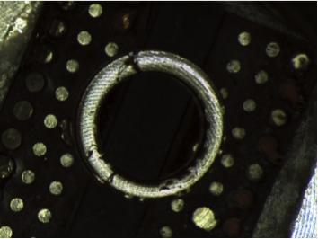
Characterisation of wire bonds (pull tests of wires with a thickness from 20 up to 400 µm, shear tests, etc.)
-
3-point and 4-point bending tests up to 1000 N for different materials (wafers, PCBs, etc.)
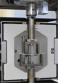
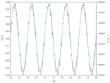
Dynamic-Mechanical Analyser
Investigations with the Dynamic-mechanical analyser give information about the viscoelastic and "rheological" properties of solids and liquids.
Our main focus/competences
- Creeping and creep recovery
- Stress relaxation
- Stress ramps
- Shear rate ramps
- Iso-deformation and iso-stress
- Fatigue strength verification (optional wave forms)
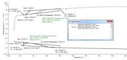
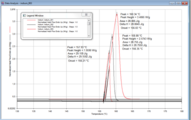
Differential Scanning Calorimetry (DSC 8000)
With differential scanning calorimetry the absorbed or emitted heat quantity of samples during heating or cooling-down can be measured. Furthermore, it is possible to describe an isothermal process.
Our main focus/competences
- Determination of reaction kinetics
-
Determination of specific heat capacity
-
Determination of melting and glass transition temperatures
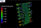
Non-destructive Failure Analysis CT
Non-destructive investigations for a multitude of materials with 2D radioscopy or 3D computed tomography.
Our main focus/competences
-
Failure analysis
-
Investigations of components and materials
-
Quantitative analysis of porosities and inclusions
-
Nominal-actual value comparisons
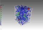
Non-destructive Failure Analysis SAM
Non-destructive investigations of components with emphasis on the detection of delaminations and cracks.
Zerstörungsfreie Untersuchungen an einer Vielzahl von Materialien mit Schwerpunkt auf der Detektion von Delaminationen und Rissen.
Our main focus/competences
- Detection of defects such as delaminations in samples built up by different materials (e.g. PCBs).
- Investigations of cracks in different materials (e.g. in PCBs or cemented carbides)
- Porosity analysis
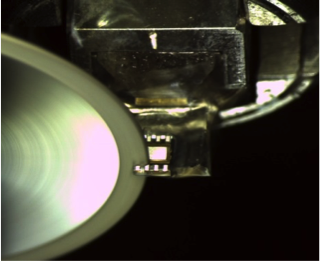
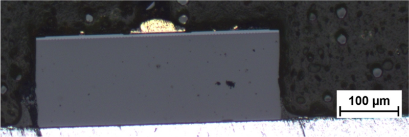
Target Preparations
We specialise in the preparation of microelectronic components for further investigations by SEM, CT, SAM, AFM or light microscopy.
Our main focus/competences
- Preparation of printed circuit boards (PCBs)
- Preparation of LED-modules/LED-chips for further investigations such as the packaging technology or wire bonds
- Preparation of TSVs (Through Silicon Vias)
- Preparation of micro hot plates for the evaluation of underetchings
- Documentation by light microscopy
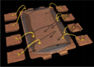
T3Ster – Thermal Impedance
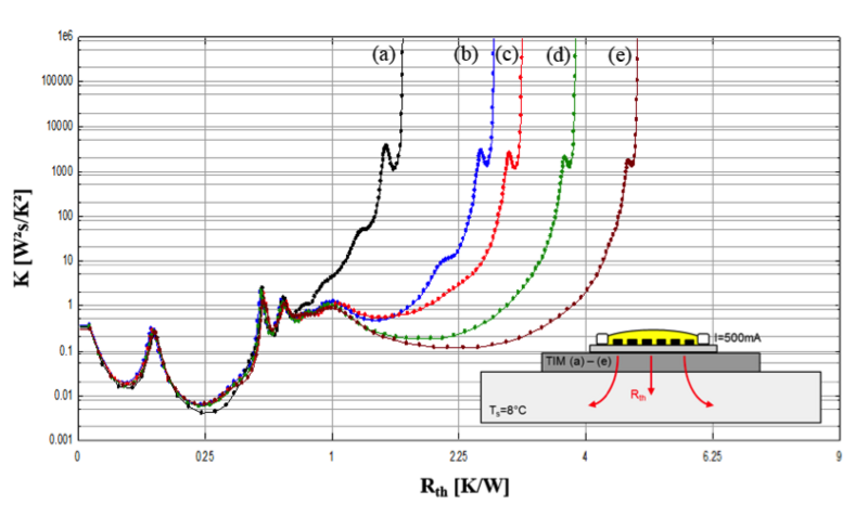
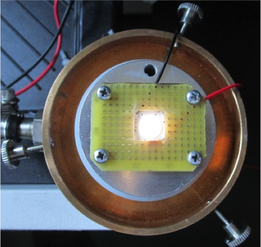
We offer the thermal characterisation of packages for semiconductor devices like integrated circuits (ICs) or Power-LEDs.
- Reconstruction of heat flows in complex electronic components
- Thermal evaluation of packages
- Thermal behaviour of 3D-integrated electronic components
- Thermal dissipation behaviour of Power-LEDs
- Failure mode analysis in-situ and non-destructive
- Verification of simulations concerning the thermal behaviour
- In-situ thermal live-mode testing of electronic components