The material characterization accompanied by simulation is used in “Non Destructive Testing” using ultrasound and also for material-parameter determination like: eigenstress, elastic constants, flow curves, fracture- and interface properties, thermal conductivity and capacities. In particular numerical modeling is used to go beyond analytical evaluation methods for micro pillar, Raman, XRD, nanoindentation etc. experiments.
Ultrasound simulation
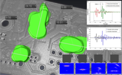
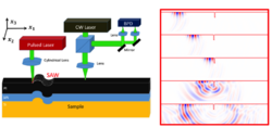
Ultrasound simulation is used to support our experimental methods: the “Scanning Acoustic Microscope (SAM)” at MCL and the “Laser Ultrasound Method” in cooperation with the Karl-Franzens-University Graz. The combination of simulation and experiments gives an advantage especially for the interpretation of complex sound wave behavior like propagation and conversion of bulk and surface waves. This enables an advanced interpretation an detection of defects in complex microelectronics components [1,2] and the characterization of elastic parameters e.g. of thin films [3,4].
One methodological focus lies in the use and development of the “Elastic Finite Integration Technique (EFIT)” capturing the behavior under strong damping, dispersion and transmission in complex microelectronics components.
Eigenstress
Eigenstresses in thin layers take on very high values (in the order of GPa). The stored elastic energy can constitute a major crack driving force. In Leoben the “Ion Layer Removal (ILR)” method was developed, which enables the determination of local and depth resolved eigenstress measurements [5]. By supportive finite element modeling (FEM), stress reconstruction is also possible in the presence of anisotropy and plasticity.
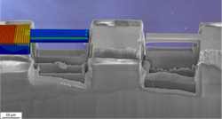
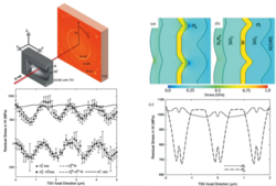
FEM is also used in combination with Raman measurements to reconstruct the complex stress-tensor field within microelectronics components, e.g. for 3D integration [6]. The simulation of layer per layer deposition, including intrinsic and thermal stress, was used to understand the stress concentrations at the scalloped wall of a tungsten Trough Silicon Via (TSV) (because of the Bosch process), which was measured by X-ray nanodiffraction [7].
Fracture- and interface-strength of thin films
Fracture and Interface toughness is strongly dependent on the microstructural design. To investigate this topic further, simulations and micro-cantilever fracture experiments are done. For this task the “Configurational Force” concept is used (see also “Damage in multi-material composits”) [8].


![Fracture experiments and simulations (using the “Configurational Force” concept) for micro-cantilevers [8].](/fileadmin/_processed_/3/e/csm_Simul_FE_Zuverlaessigkeit8_fee78781da.png)